(China (Mainland))


Product Summary
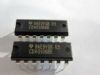
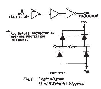
The CD40106BE is a CMOS hex schmitt trigger. The applciations of the CD40106BE include wave and pulse shapers, high-noise-environment system, monostable multivibtators, astable multivibrators.
Parametrics
CD40106BE absolute maximum ratings: (1)DC supply-voltaqe range, (Vdd) Voltoges referenced to Vss Terminal): -0.5V to +20V; (2)Input voltage range, all inputs: -0.5V to VDD +0.5V; (3)DC input current, any one INPUT: ±10mA; (4)POWER DISSIPATION PER PACKAGE (PD), For TA = -55℃ to +100℃: 500mW; For TA = +100℃ to +125℃: Derate Linearity at 12mW/℃ to 200mW; (5)Device dissipation per outputtransistor, For TA = fuu package-temperature range (All Package Types): 10OmW; (6)Operatinq-temperaturi range(TA): -55℃ to + 125℃; (7)Storage temperature range (Tstg): -65℃ to +150℃; (8)Lead temperature (during soldering): At distance 1/16 ± 1/32 Inch (1.59 ± 0.79mm) from case for 10s max: +265℃.
Features
CD40106BE features: (1)Schtnitt-tHgger action with no externa) component; (2)Hysteresis voltage (typ.) 0.9 V at VDD=5 V, 2.3 V at Vdd = 10 V, and 3.5 V at Vdd = 15 V; (3)Noise immunity greater than 50%; (4)No limit on input rise and fall times; (5)Standardized, symmetrical output characteristics; (6)100% tested for quiescent current at 20 V; (7)Maximum input current of 1 mA at 18 V over full package-temperature range; 100 nA at 18 V and 25℃; (8)Low Vdd to Vss current during slow input ramp; (9)5-V, 10-V, and 15-V parametric ratings; (10)Meets all requirenments of JEDEC Tentative Standard No. 13B, "Standard Specifications for Description of "B" Series CMOS Devlcet".
Diagrams
| Image | Part No | Mfg | Description |  |
Pricing (USD) |
Quantity | ||||||||||||
|---|---|---|---|---|---|---|---|---|---|---|---|---|---|---|---|---|---|---|
 |
 CD40106BE |
Texas Instruments |
Inverters Hex Schmitt Trigger |
Data Sheet |
|
|
||||||||||||
|
CD40106BEE4 |
Texas Instruments |
Inverters Hex Schmitt Trigger |
Data Sheet |
|
|
||||||||||||