(China (Mainland))


Product Summary
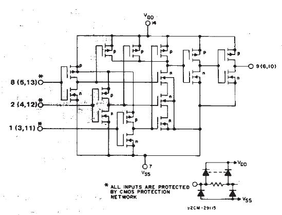
The CD4075BE is a CMOS OR gate. The device provides the system designer with direct implementation of the positive-logic OR function and supplement the existing family of CMOS gates. The CD4075BE is supplied in 14-lead dual-in-line ceramic packages (D and F suffixes), 14-lead dual-in-tine plastic packages (E suffix), and in chip form (H suffix).
Parametrics
CD4075BE absolute maximum ratings: (1)DC supply-voltaqe range, (Vdd) Voltoges referenced to Vgs Terminal): -0.5V to +20V; (2)Input voltage range, all inputs: -0.5V to VDD +0.5V; (3)DC input current, any one INPUT: ±10mA; (4)POWER DISSIPATION PER PACKAGE (PD), For TA = -55℃ to +100℃: 500mW; For TA = +100℃ to +125℃: Derate Linearity at 12mW/℃ to 200mW; (5)Device dissipation per outputtransistor, For TA = fuu package-temperature range (All Package Types): 10OmW; (6)Operatinq-temperaturi range(TA): -55℃ to + 125℃; (7)Storage temperature range (Tstg): -65℃ to +150℃; (8)Lead temperature (during soldering): At distance 1/16 ± 1/32 Inch (1.59 ± 0.79mm) from case for 10s max: +265℃.
Features
CD4075BE features: (1)Medium-Speed Operation-tpLH, tpHL = 60 ns (typ.) at VDD = 10 V; (2)100% tested for qi|iescent current at 20 V; (3)Maximum input current of 1 at 18 V over full pockage-temperature range; 100 nA at 18 V and 25℃; (4)Standardized, tymmetricaJ output characteristict; (5)Noise margin (over full package tsmperature range), 1V at VDD= 5 V; 2V at VDD = 10 V; 2.5 V at Vdd = 15 V; (6)5-V, 10-V, and 15-V parametric ratings; (7)Meets all requirements of JEDEO Tentative Standard No. 13B, "Standard Specifications for Description of Series CMOS Devices".
Diagrams
| Image | Part No | Mfg | Description |  |
Pricing (USD) |
Quantity | ||||||||||||
|---|---|---|---|---|---|---|---|---|---|---|---|---|---|---|---|---|---|---|
 |
 CD4075BE |
Texas Instruments |
Gates (AND / NAND / OR / NOR) Triple 3-Input. |
Data Sheet |
|
|
||||||||||||
|
CD4075BEE4 |
Texas Instruments |
Gates (AND / NAND / OR / NOR) Triple 3-Input. |
Data Sheet |
|
|
||||||||||||