(China (Mainland))

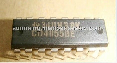
Product Summary
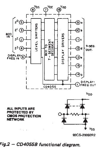
The CD4055BE is a CMOS liquid-crystal display driver. The CD4055BE is a single-digit BCD to-7-segment decoder/driver circuits that provide level-shifting functions on the chip. This feature permits the BCD input-signal swings (Vdd to VSS) to be the same as or different from the 7-segment output-signal swings (VDD to For example, the BCD input-signal swings (VDD to VSS) may be as small as 0 to 3 V, whereas the output-display drive-signal swing (VDD to VSS) may be as large as from 0 to 15V.
Parametrics
CD4055BE absolute maximum ratings: (1)DC supply-voltaqe range. (VDD) Voltagea referenced to Vss Terminal: -0.5V to +20V; (2)Input voltage range, all inputs: -0.5V to VDD +0.5V; (3)DC input current, any one input: ±10mA; (4)Power dissipation per package (PD): For TA= -55℃ to +100℃: 500mW; (5)For Ta = +100℃ to +125℃: Derate Linearity at 12mW/℃ to 200mW; (6)Device dissipation per output transistor, for Ta = FULL PACKAGE-temperature range (all package types): 100mW; (7)Operating-temperature range (TA): -55℃ to +125℃; (8)Storage temperature range(Tstfl): -65℃ to +150℃; (9)Lead temperature (during soldering): At distance 1/16 ± 1/32 inch (1.59 ± 0.79mm) from case for 10s max: +265℃.
Features
CD4055BE features: (1)Operation of liquid crystals with CMOS ciftuits provides ultra-Low-power dhplays; (2)Equivalent ac output drive for liquid-crystal displays-no external capacitor required; (3)Voltage doubling across display, e.g. ; (4)Low- or hjgh-output level dc drive for other types of displays; (5)On-chip logic-leveJ conversion for different input- and output-level swings; (6)Full decoding of all input combinations: 0-9, L, H, P, A,- and blank positions; (7)Strobed-latch functionCD4054B Series and CD4056B Series; (8)DISPLAY-FREQUENCY (DF) output for liquid-crystal common-line drive signal CD4055B Series {CD4054B Series also: introductory text); (9)100% tested for quiescent current at 20 V; (10)Maximum input current of 1 at 18 V over full package temperature range; 100 nA at 18 V and 25C; (11)Noise margin (over full package temperature range):; (12)1 V at Vdd = 5 V 2Vat Vdd = 10 V 2.5 V at Vpp = 15 V; (13)5-V, 10-V, and 15-V parametric ratings.
Diagrams
| Image | Part No | Mfg | Description |  |
Pricing (USD) |
Quantity | ||||||||||||
|---|---|---|---|---|---|---|---|---|---|---|---|---|---|---|---|---|---|---|
 |
 CD4055BE |
Texas Instruments |
LCD Drivers BCD to 7 Segment |
Data Sheet |
|
|
||||||||||||
|
CD4055BEE4 |
Texas Instruments |
LCD Drivers BCD to 7 Segment |
Data Sheet |
|
|
||||||||||||